Anti-static peek in the semiconductor field static elimination components applications
2025-06-30 17:00:24
As semiconductor technology continues to advance, the requirements for controlling electrostatic discharge during production are becoming more stringent. Damage to semiconductor equipment and components from electrostatic discharge (ESD) may not only lead to production standstill, but also affect product quality and reliability. Therefore, how to effectively eliminate static electricity has become an important challenge for the semiconductor industry. In this context, anti-static PEEK (polyether ether ketone) materials have become indispensable in static elimination components due to their excellent electrical properties and high temperature resistance.
Characteristics of anti-static PEEK
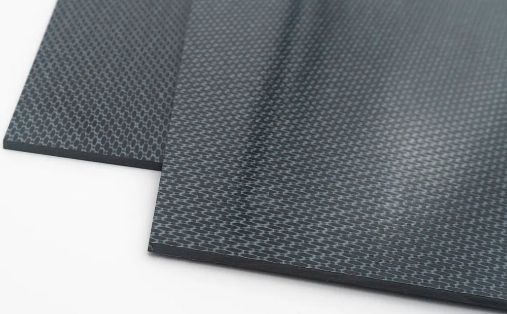
As a high-performance Engineering Plastic, PEEK has excellent mechanical properties, high temperature resistance, corrosion resistance and good electrical insulation properties. In order to cope with the stringent requirements of the semiconductor industry with regard to static electricity, PEEK materials can be made antistatic by adding conductive fillers (such as carbon fibre or graphite) to regulate their surface resistance. This allows PEEK to excel in static sensitive environments, especially in cleanroom environments.
In addition, PEEK has excellent thermal stability and chemical resistance, enabling it to work stably for long periods of time at high temperatures and in highly corrosive environments. This is critical for the high-temperature, precision operating requirements common in semiconductor manufacturing processes.
Anti-static PEEK in semiconductor applications
In semiconductor production, the application of anti-static PEEK is mainly reflected in the following aspects:
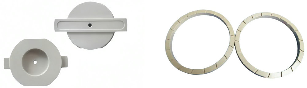
Wafer trays and fixtures: wafers are one of the most critical components in the semiconductor manufacturing process, PEEK materials are widely used in wafer trays and fixtures, not only to effectively eliminate static electricity, but also in the transport and storage process to prevent static electricity on the surface of the wafers caused by damage.
Test sockets and connectors: In the test process of semiconductor components, anti-static PEEK materials are commonly used in the manufacture of test sockets, test fixtures and connectors. It can effectively avoid static electricity on the test equipment and components caused by interference, to ensure the accuracy of the test and component safety.
Cleanroom equipment: Semiconductor production has very high requirements for cleanrooms. The excellent performance of anti-static PEEK makes it an indispensable material in cleanrooms. Whether it is production equipment, transmission devices, or operating tools, PEEK provides effective static elimination and avoids static contamination of the environment.
Conclusion
With the increasing sophistication and complexity of semiconductor manufacturing technology, the requirements for static electricity management are getting higher and higher. Anti-static PEEK materials have become an important choice for static elimination components in the semiconductor field due to their excellent electrical properties, high temperature resistance, and high corrosion resistance. In the future, with the semiconductor industry's demand for higher quality and higher performance, the application of anti-static PEEK will be further promoted and developed in more fields.